Printed circuit board design:
Our in-house PCB designers specialise in designing printed circuit boards for semi-conductor test for many of the worlds’ largest Integrated Device Manufacturers (IDMs); we aim to understand our customers’ needs and follow best-practice approaches, adhering to IPC Generic Standards for Printed Circuit Board Design in conjunction with IPC standards for PCB Manufacturing.
Our customers’ designs are often time-critical applications, so, where applicable, our team of PCB design engineers work closely with our manufacturing group to highlight the complete product development lifecycle in order for us to provide accurate product delivery timescales. This proven model allows ITE to deliver the first article right first time, thus our customers’ innovations to come to fruition in the shortest timescales.
We listen to our customers and are committed to quality processes that continually improve our internal processes, and, the service and product we supply. ITE are compliant to ISO 9001:2008, WEE and RoHS, and, we have experience in complying to specific company standards.
We understand IDM’s can naturally be anxious about outsourcing designs to an external business, primarily because of the fear of high external expenditure, coupled with the loss of internal control associated with outsourcing, but, we at ITE are confident that our customers are often pleasantly surprised in costs involved in outsourcing design and manufacture with ITE, we are told customers think of ITE as a ‘No headaches supplier’, and, customers are happy to provide references on our services.
PCB Design Tools:
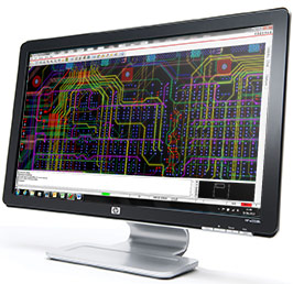
ITE use Cadence Allegro (www.cadence.com) and ORCAD CAD tools, and, have purchased multiple seats/licences that we continue to maintain; consequently we are not restricted to specific versions of Allegro. We have decades of experience in a wide range of disciplines of which a summary is shown below:
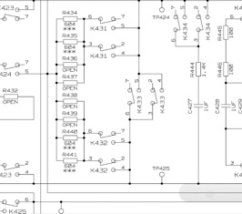
- Schematic Capture (ORCAD Capture and Cadence HDL)
- MCAD bi-directional interface via .idf transfer
- Multi-site
- Multi-layer (up to 32 layers)
- High speed digital
- Matched
- Impedance
- Length
- Co-planar (and broadside)
- Stripline
- Microstrip
- Differential
- Use and recommendations of RF and high speed dielectric materials
- Use and recommendations high temperature/high Tg materials (and components)
- High voltage and high current applications
- PTH, blind and buried and backdrilled vias
- Design check/DRC
- Autorouting (where allowable)
- Gerber 274X, 274D Artwork Output
- Valor ODB++ File Output


